找仪器
企业性质一般经销商
入驻年限第5年
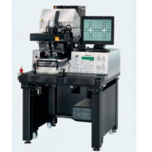
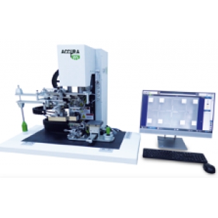
MA/BA6
Perfect Low-Cost Solution:
• High Accuracy
• Good Optical performance
• latest processes (e.g. UV-NIL)
Addressed Markets:
• MEMS
• Telecommunications
• Compound Semiconductors
• Nano Imprint Lithography
Technical Data
• Wafer size: up to 150 mm / 6′′ (round)
• Min. pieces: 5 x 5mm
• Mask size: SEMI spec, standard up to 7′′ x 7′′ (SEMI)
Exposure Modes
• Contact: soft, hard, low vacuum, vacuum
• Proximity : exposure gap 1-300 μm
Optics
• UV250, UV300, UV400 and broadband optics
• Intensity Uniformity ± 5% on 100mm
• Constant power or constant intensity
• Lamp sizes: 200W, 350W, 500W (for UV250)
• Resolution down to 0,4 μm L/S (vacuum contact, UV250)
Alignment
• Top Side Alignment (TSA); Bottom Side Alignment (BSA); Infrared Alignment (IR) Vacuum
• TSA alignment accuracy: 0.5μm (with SUSS recommended wafer targets)
• BSA:down to 1μm
• Alignment gap:1–1000μm

 热线电话
热线电话