Perfect Low-Cost Solution:
• High Accuracy
• Good Optical performance
• latest processes (e.g. UV-NIL)
Addressed Markets:
• MEMS
• Telecommunications
• Compound Semiconductors
• Nano Imprint Lithography
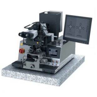
Manual Tool: Easy To Operate
Technical Data
• Wafer size: 1′′ up to 100 mm / 4′′ (round)
• Min. pieces: 5 x 5 mm
• Wafer thickness: up to 4 mm
• Mask size: standard 2′′ x 2′′ up to 5′′ x 5′′ (SEMI)
• Mask thickness: up to 4.8 mm / 190 mil
Exposure Modes
• Contact: soft, hard, vacuum, soft vacuum
• Proximity up to 50μm gap
Optics
• UV250, UV300, UV400 and broadband optics
• Intensity Uniformity ± 3% on 100mm
• Constant power or constant intensity
• Lamp sizes: 200W, 350W, 500W (for UV250)
• Resolution down to 0,5 μm L/S (vacuum contact, UV250)
Alignment
• TSA alignment accuracy: 0.5μm (with SUSS recommended wafer targets)
• Transmitted IR Alignment accuracy: < 5μm (<2μm under special process conditions)
• Alignment gap:10–50μm
Single or splitfield microscope with/w/o CCD camera
香港壘為信息科技實業有限公司
仪器网(yiqi.com)--仪器行业网络宣传传媒
 热线电话
热线电话