2019年:[1] Leonardi F, Zhang Q, Kim Y H, et al. Solution-sheared thin films of a donor-acceptor random copolymer/polystyrene blend as active material in field-effect transistors[J]. Materials Science in Semiconductor Processing, 2019, 93: 105-110.
[2] Mortet V, Drbohlavova L, Lambert N, et al. Conductivity of boron-doped diamond at high electrical field[J]. Diamond and Related Materials, 2019, 98: 107476.
[3] Armistead F J, De Pablo J G, Gadêlha H, et al. Cells Under Stress: An Inertial-Shear Microfluidic Determination of Cell Behavior[J]. Biophysical journal, 2019, 116(6): 1127-1135.
[4] Salzillo T, Campos A, Mas-Torrent M. Solution-processed thin films of a charge transfer complex for ambipolar field-effect transistors[J]. Journal of Materials Chemistry C, 2019, 7(33): 10257-10263.
[5] Chen H, Liu G, Zhang S, et al. Fundus-simulating phantom for calibration of retinal vessel oximetry devices[J]. Applied optics, 2019, 58(14): 3877-3885.
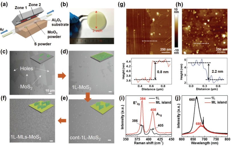
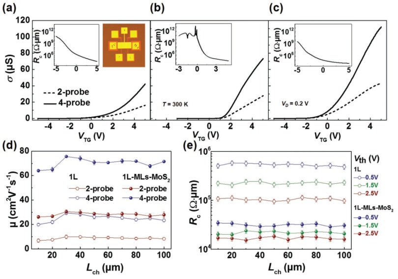
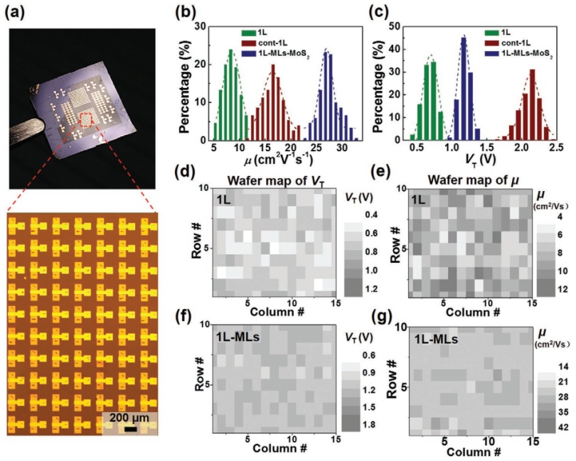
[6] Zhang S, Xu H, Liao F, et al. Wafer-scale transferred multilayer MoS2 for high performance field effect transistors[J]. Nanotechnology, 2019, 30(17): 174002.
[7] Martin E L, Bryan M T, Pagliara S, et al. Advanced Processing of Micropatterned Elasto-Magnetic Membranes[J]. IEEE Transactions on Magnetics, 2019.
[8] Liu J, Singh A, Llandro J, et al. A low-temperature Kerr effect microscope for the simultaneous magneto-optic and magneto-transport study of magnetic topological insulators[J]. Measurement Science and Technology, 2019.
[9] Ye K, Liu L, Liu Y, et al. Lateral Bilayer MoS2–WS2 Heterostructure Photodetectors with High Responsivity and Detectivity[J]. Advanced Optical Materials, 2019: 1900815.
[10] Gilboa T, Zvuloni E, Zrehen A, et al. Automated, Ultra‐Fast Laser‐Drilling of Nanometer Scale Pores and Nanopore Arrays in Aqueous Solutions[J]. Advanced Functional Materials, 2019: 1900642.
[11] You H, Zhuo Z, Lu X, et al. 1T′-MoTe2-Based On-Chip Electrocatalytic Microdevice: A Platform to Unravel Oxidation-Dependent Electrocatalysis[J]. CCS Chemistry, 2019: 396-406.
[12] Fan X, Wei G, Lin X, et al. Phase-Change Based Interlayer Exchange Coupling Control[J]. arXiv preprint arXiv:1907.10784, 2019.
[13]Zhang Q, Leonardi F, Pfattner R, et al. A Solid‐State Aqueous Electrolyte‐Gated Field‐Effect Transistor as a Low‐Voltage Operation Pressure‐Sensitive Platform[J]. Advanced Materials Interfaces, 2019: 1900719.
[14] Yang R, Liu L, Feng S, et al. One-Step Growth of Spatially Graded Mo1-xWxS2 Monolayer with Wide Span in Composition (from x= 0 to 1) at Large Scale[J]. ACS applied materials & interfaces, 2019.
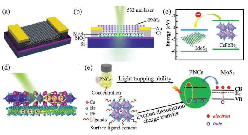
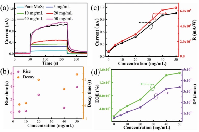
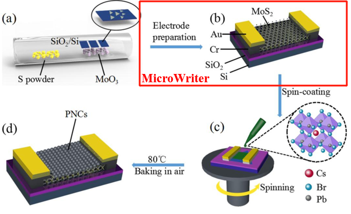
[15] Zhang L, Shen S, Li M, et al. Strategies for Air‐Stable and Tunable Monolayer MoS2‐Based Hybrid Photodetectors with High Performance by Regulating the Fully Inorganic Trihalide Perovskite Nanocrystals[J]. Advanced Optical Materials, 2019: 1801744.
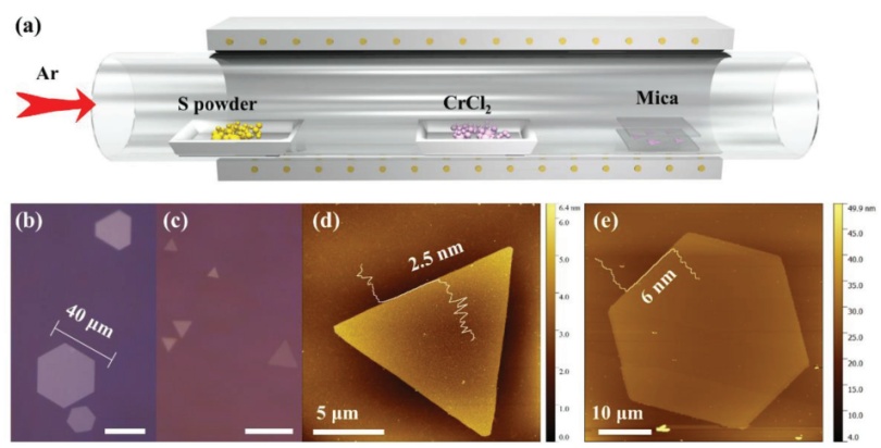
[16] Zhou S, Wang R, Han J, et al. Ultrathin Non‐van der Waals Magnetic Rhombohedral Cr2S3: Space‐Confined Chemical Vapor Deposition Synthesis and Raman Scattering Investigation[J]. Advanced Functional Materials, 2019, 29(3): 1805880.
[17] Chen Y, Casals B, Sanchez F, et al. Solid-State Synapses Modulated by Wavelength-Sensitive Temporal Correlations in Optic Sensory Inputs[J]. ACS Applied Electronic Materials, 2019.
[18] Gu Y, Oliferenko S. Cellular geometry scaling ensures robust division site positioning[J]. Nature communications, 2019, 10(1): 268.
2018年:[1] Wei G, Lin X, Si Z, et al. Optical control of magnetism in NiFe/VO2 heterostructures[J]. arXiv preprint arXiv:1805.02453, 2018.
[2] Davydova M, Taylor A, Hubík P, et al. Characteristics of zirconium and niobium contacts on boron-doped diamond[J]. Diamond and Related Materials, 2018, 83: 184-189.
[3] Campos A, Riera-Galindo S, Puigdollers J, et al. Reduction of charge traps and stability enhancement in solution-processed organic field-effect transistors based on a blended n-type semiconductor[J]. ACS applied materials & interfaces, 2018, 10(18): 15952-15961.
[4] Jia Z, Hu W, Xiang J, et al. Grain wall boundaries in centimeter-scale continuous monolayer WS2 film grown by chemical vapor deposition[J]. Nanotechnology, 2018, 29(25): 255705.
[5]Tarn M D, Sikora S N F, Porter G C E, et al. The study of atmospheric ice-nucleating particles via microfluidically generated droplets[J]. Microfluidics and nanofluidics, 2018, 22(5): 52.
[6] Jin B, Huang P, Zhang Q, et al. Self‐Limited Epitaxial Growth of Ultrathin Nonlayered CdS Flakes for High‐Performance Photodetectors[J]. Advanced Functional Materials, 2018, 28(20): 1800181.
[7] Vallès F, Palau A, Rouco V, et al. Angular flux creep contributions in YBa2Cu3O7−δ nanocomposites from electrical transport measurements[J]. Scientific reports, 2018, 8(1): 5924.
[8] Lόpez-Mir L, Frontera C, Aramberri H, et al. Anisotropic sensor and memory device with a ferromagnetic tunnel barrier as the only magnetic element[J]. Scientific reports, 2018, 8(1): 861.
[9] Xu H, Zhang H, Guo Z, et al. High‐Performance Wafer‐Scale MoS2 Transistors toward Practical Application[J]. Small, 2018, 14(48): 1803465.

 RSR1000旋转遮光式太阳能测量评估系统

 评论
评论